
Ứng dụng của Thị giác Máy tính trong Kiểm tra Mối hàn
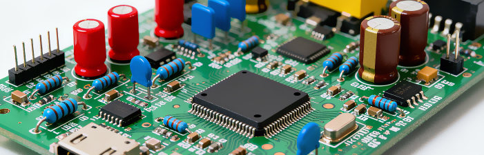
Trong ngành sản xuất điện tử luôn phát triển nhanh chóng, chất lượng các mối hàn không chỉ là một chi tiết nhỏ—mà chính là yếu tố then chốt quyết định độ tin cậy và hiệu suất lâu dài của sản phẩm. Các mối hàn đóng vai trò như xương sống vô hình của các bảng mạch in (PCB), tạo nên các kết nối điện và cơ học quan trọng giữa các linh kiện như điện trở, tụ điện và vi mạch. Một mối hàn bị lỗi duy nhất—dù là mối hàn nguội không dẫn điện đúng cách, một khoảng rỗng làm giảm độ bền cấu trúc, hay hiện tượng nối tắt gây đoản mạch—đều có thể dẫn đến hậu quả nghiêm trọng.
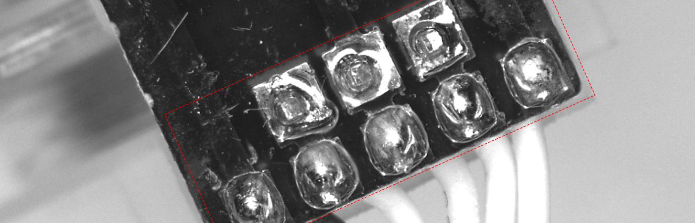
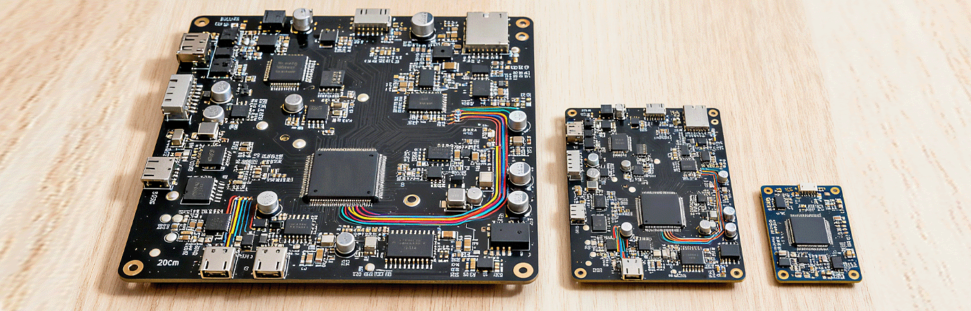
Khi các thiết bị điện tử tiếp tục thu nhỏ kích thước—với các linh kiện giờ đây nhỏ đến mức 01005 (0,4mm x 0,2mm) và các mạch in (PCB) ngày càng dày đặc hơn với hàng nghìn mối hàn được gói gọn trong không gian nhỏ hẹp—các phương pháp kiểm tra truyền thống đã chứng minh ngày càng không đủ hiệu quả. Người vận hành nhanh chóng bị mệt mỏi khi phải kiểm tra hàng trăm hoặc hàng nghìn mối hàn mỗi giờ, dẫn đến sự đánh giá thiếu nhất quán: một mối hàn có phần viền thiếc hơi không đều có thể được chấp nhận bởi người này nhưng lại bị từ chối bởi người khác. Sự chủ quan này không chỉ làm tăng nguy cơ để sản phẩm lỗi đến tay người tiêu dùng mà còn gây lãng phí tài nguyên do phải sửa chữa không cần thiết những mối hàn.
Một hệ thống thị giác máy để kiểm tra mối hàn chì là sự kết hợp được thiết kế cẩn thận giữa phần cứng và phần mềm, trong đó từng thành phần hoạt động đồng bộ nhằm mô phỏng và vượt trội hơn khả năng thị giác của con người. Về phía phần cứng, các thành phần chính của hệ thống bao gồm các camera độ phân giải cao, thiết lập chiếu sáng chuyên dụng, ống kính chính xác và một bộ xử lý mạnh mẽ. Chiếu sáng có lẽ là thành phần phần cứng ít được đánh giá đúng mức nhất nhưng lại cực kỳ quan trọng: khác với ánh sáng nhà xưởng thông thường, loại ánh sáng này có thể tạo ra hiện tượng lóa trên các bề mặt hàn bóng hoặc tạo bóng đổ che khuất chi tiết, trong khi thị giác máy sử dụng các giải pháp được điều chỉnh phù hợp. Ví dụ, chiếu sáng đồng trục phát ra ánh sáng dọc theo cùng trục với ống kính camera, giảm thiểu phản xạ trên mối hàn chì và giúp dễ dàng phát hiện các khoảng rỗng. Đèn vòng, với thiết kế hình tròn, cung cấp ánh sáng đồng đều trên toàn bộ bảng mạch in (PCB), đảm bảo chất lượng hình ảnh ổn định ngay cả đối với các mối nối ở mép bảng.
Các camera, đồng thời, được chọn dựa trên nhu cầu độ chính xác của quá trình kiểm tra. Đối với các linh kiện mạch in tiêu chuẩn, một camera từ 2–5 megapixel (MP) là đủ, nhưng đối với các mối hàn vi mô trong thiết bị y tế hoặc điện tử hàng không vũ trụ, các camera 10–20 MP kết hợp với ống kính phóng đại cao (lên đến 100x) là cần thiết để ghi lại các chi tiết nhỏ tới 1–2 micromet. Các hình ảnh đã chụp sau đó được gửi đến một bộ xử lý—thường là một máy tính công nghiệp chuyên dụng hoặc hệ thống nhúng—nơi phần mềm sẽ thực hiện xử lý tiếp theo.
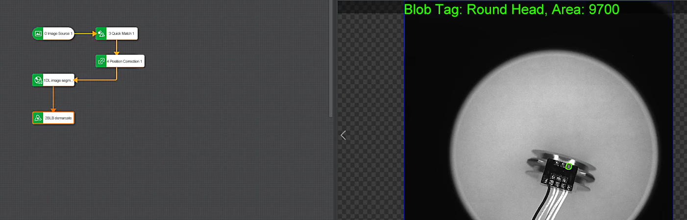
Phần mềm là "bộ não" của hệ thống thị giác máy, và khả năng của nó đã tiến bộ vượt bậc cùng với sự phát triển của học máy (ML) và học sâu (DL). Các kỹ thuật xử lý ảnh truyền thống, như phát hiện biên (để xác định ranh giới của mối hàn thiếc) và ngưỡng hóa (để phân biệt thiếc hàn với các pad trên mạch in PCB), vẫn đóng vai trò trong việc trích xuất đặc trưng. Ví dụ, một mạng thần kinh tích chập (CNN) có thể phân biệt giữa một mối hàn thiếc bình thường và một mối hàn có lỗ rỗng 5 micromet—một điều mà ngay cả các thao tác viên được đào tạo cũng có thể bỏ sót—bằng cách phân tích những biến đổi tinh vi về màu sắc, kết cấu và hình dạng. Sau khi phân tích, hệ thống sẽ phân loại mỗi mối nối là "đạt" hoặc "không đạt" dựa trên các tiêu chuẩn chất lượng đã định trước và tạo ra báo cáo chi tiết, đánh dấu vị trí và loại lỗi để kỹ sư xem xét.
Những lợi thế của thị giác máy so với các phương pháp truyền thống vừa rõ rệt vừa có thể đo lường được. Thứ nhất, độ chính xác và chính xác là không thể so sánh: các hệ thống thị giác máy có thể phát hiện các khuyết tật nhỏ tới 1 micromet, vượt xa giới hạn 20–30 micromet của thị giác con người (ngay cả khi dùng kính lúp). Thứ hai, độ Nhất loại bỏ sự biến đổi do con người: hệ thống áp dụng cùng một tiêu chí chất lượng cho mọi mối hàn, mỗi lần như nhau, đảm bảo rằng một mối hàn được kiểm tra trong ca đêm sẽ được đánh giá theo đúng tiêu chuẩn như khi kiểm tra trong ca ngày. Thứ ba, tốc độ tăng hiệu quả sản xuất: một hệ thống thị giác máy điển hình có thể kiểm tra 10.000 mối hàn trên một bo mạch in (PCB) trong vòng chưa đến 10 giây — công việc này sẽ mất một nhân viên vận hành từ 5 đến 10 phút. Cuối cùng, nhận Định Dựa Trên Dữ Liệu cho phép cải tiến liên tục: hệ thống ghi lại mọi kết quả kiểm tra, cho phép các nhà sản xuất theo dõi xu hướng khuyết tật theo thời gian.
Tính linh hoạt của thị giác máy đã khiến nó trở nên không thể thiếu trong nhiều ngành công nghiệp. Trong lĩnh vực lĩnh vực ô tô , nơi các mạch in (PCB) cung cấp năng lượng cho các hệ thống quan trọng như Bộ điều khiển động cơ (ECUs) và Hệ thống Hỗ trợ Lái xe Nâng cao (ADAS), thị giác máy đảm bảo an toàn. Một mối nối lỗi trong mô-đun radar ADAS có thể khiến hệ thống phát hiện sai chướng ngại vật, dẫn đến tai nạn.
Mặc dù đã đạt được nhiều thành công, thị giác máy vẫn đối mặt với những thách thức kéo dài. Một trở ngại lớn là thiết kế mạch in (PCB) phức tạp : khi các linh kiện trở nên nhỏ hơn và các mạch in được bố trí dày đặc hơn, các linh kiện chồng lấn hoặc các khu vực bị che khuất có thể làm mờ các mối nối, khiến camera khó ghi lại hình ảnh rõ ràng. Để giải quyết vấn đề này, các nhà sản xuất đang phát triển các hệ thống đa camera chụp hình từ 2–4 góc độ, đảm bảo không bỏ sót bất kỳ mối nối nào. Thách thức khác là dữ liệu huấn luyện : Các thuật toán ML/DL cần các bộ dữ liệu lớn và chất lượng cao để hoạt động hiệu quả, nhưng việc tạo ra các bộ dữ liệu này tốn nhiều thời gian—việc gắn nhãn 10.000 hình ảnh lỗi có thể kéo dài hàng tuần. Hiện nay, các nhà nghiên cứu đang sử dụng phương pháp tạo dữ liệu tổng hợp, trong đó các mô hình máy tính tạo ra những hình ảnh thực tế về các mối hàn (kể cả các lỗi hiếm gặp), nhằm giảm sự phụ thuộc vào dữ liệu thực tế.
Trong tương lai, một số xu hướng sẽ định hình tương lai của thị giác máy trong kiểm tra mối hàn. Tích hợp AI với robot sẽ cho phép sửa chữa ngay lập tức: nếu hệ thống thị giác máy phát hiện thiếu mối hàn, cánh tay robot sẽ ngay lập tức bổ sung thêm thiếc hàn, loại bỏ nhu cầu can thiệp thủ công và giảm thời gian ngừng sản xuất từ 20–30%. thị giác máy móc 3D sẽ trở nên phổ biến hơn: khác với các hệ thống 2D chỉ ghi lại chi tiết bề mặt, các hệ thống 3D sử dụng quét ánh sáng cấu trúc để tạo mô hình 3D của các mối nối, giúp dễ dàng đo thể tích thiếc hàn và phát hiện các lỗi như thiếu thiếc. Tích hợp IoT sẽ cho phép giám sát từ xa: các nhà sản xuất có thể theo dõi dữ liệu kiểm tra trong thời gian thực từ bất cứ đâu, sử dụng các nền tảng dựa trên đám mây để xác định các vấn đề (ví dụ, máy ảnh mất nét) và gửi cảnh báo cho các nhóm bảo trì trước khi ngừng sản xuất.
Kết luận, thị giác máy đã cách mạng hóa việc kiểm tra khớp hàn, giải quyết những hạn chế của các phương pháp truyền thống và đáp ứng nhu cầu của sản xuất điện tử hiện đại. Khả năng cung cấp độ chính xác, nhất quán, tốc độ và thông tin chi tiết đã làm cho nó trở thành nền tảng của kiểm soát chất lượng trên khắp các ngành công nghiệp. Khi các thiết bị điện tử tiếp tục nhỏ hơn và phức tạp hơn, thị giác máy sẽ trở nên quan trọng hơn để thúc đẩy đổi mới, cải thiện độ tin cậy sản phẩm và giúp các nhà sản xuất duy trì tính cạnh tranh trên thị trường toàn cầu.