

Best SWIR Camera Applications in Semiconductor & Electronics
For semiconductor fabs, electronics OEMs, and system integrators, the SWIR camera is a transformative non-destructive inspection technology that addresses the most critical quality control challenges in advanced node production.
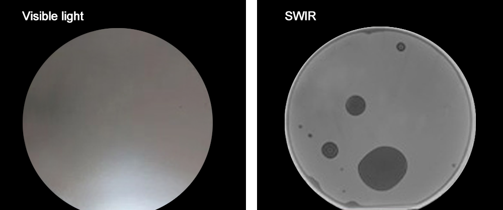
Subsurface Wafer Inspection with SWIR Cameras
Why Silicon Is Transparent in SWIR: Enabling Non-Destructive Imaging Below the Surface
Silicon wafers become optically transparent in the short-wave infrared (SWIR) spectrum between 1000–1700 nm due to their electronic bandgap (~1.12 eV). Photons in this range lack sufficient energy to excite electrons across the gap, enabling deep, non-destructive subsurface imaging—unlike visible or near-infrared light, which silicon strongly absorbs. This property allows production teams to visualize internal defects such as crystal dislocations, impurity clusters, and micro-voids without physical sectioning. As a result, material waste is reduced by ~25% compared to destructive testing methods, while preserving wafer integrity for downstream processing.
Optimal Wavelengths (1000–1700 nm) for High-Contrast, Damage-Free Defect Detection
Wavelength selection directly governs penetration depth, resolution, and contrast. Shorter SWIR wavelengths (1000–1300 nm) offer higher spatial resolution—ideal for detecting near-surface cracks under 10 μm—while longer wavelengths (1400–1700 nm) penetrate deeper into bulk silicon to reveal subsurface voids and delaminations. The 1550 nm band delivers an optimal balance: it provides 4× greater contrast for micro-fractures and voids than visible-light systems and causes zero photon-induced stress to nanostructures—unlike UV-based inspection, which risks lattice damage.
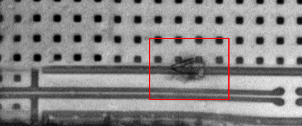
Real-World Validation: 1550 nm Line-Scan SWIR Camera Identifies Sub-Surface Cracks in 300 mm Wafers
A leading manufacturer deployed a 1550 nm line-scan SWIR camera system for high-throughput inspection of 300 mm wafers. Operating at 200 wafers/hour, the system detected subsurface micro-cracks as small as 3 μm—originating from thermal stress during rapid annealing—with a 90% detection rate improvement over conventional surface-only methods. Critically, these defects were invisible to optical and laser-scatter tools but accounted for 37% of field returns in advanced logic chips, underscoring SWIR’s role in preventing latent failures before packaging.
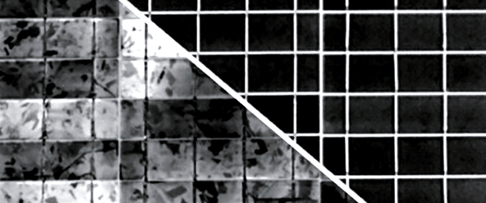
Micro-Defect Detection Using SWIR Camera Imaging
Enhanced Contrast for Sub-Micron Contaminants and Pattern Deviations on Oxide Layers
SWIR cameras detect sub-micron contaminants and pattern deviations on silicon dioxide layers with exceptional sensitivity. Because silicon remains transparent across 1000–1700 nm, SWIR imaging captures high-contrast reflectance anomalies from particulate residues, thin-film thickness variations, and lithographic misalignments—revealing features as small as 0.2 µm. This non-destructive capability replaces chemical etching for defect verification in front-end processes, reducing wafer scrap rates by 15–22%. Oxide irregularities—such as over-etching or incomplete hard-bake—alter local reflectance signatures, allowing real-time, inline identification without disrupting throughput.
Stress & Absorption Mapping via Reflectance Anomalies at 1310 nm
At 1310 nm, SWIR cameras map mechanical stress and absorption gradients through quantitative reflectance analysis. Strained lattice regions—like those around copper interconnects or dielectric interfaces—scatter photons differently, producing measurable intensity drops of 12–18% in reflectance maps. These anomalies pinpoint early-stage micro-cracks and interfacial delamination before electrical failure occurs. Similarly, absorption variations in low-k dielectrics expose voids >3 µm, enabling targeted rework. Compared to conventional thermal testing, this approach reduces packaging-related yield loss by up to 30%.
SWIR Camera Solutions for Packaging Integrity Assessment
Transmissive Behavior of Epoxy and Mold Compounds Enables Encapsulation Void Detection
Epoxy resins and mold compounds—opaque in visible light—are partially transmissive in the SWIR band (900–1700 nm), allowing non-destructive inspection of encapsulated structures. SWIR imaging detects sub-surface voids and delamination as small as 10 µm within molded packages by leveraging differential absorption contrast. Undetected, these defects reduce localized thermal conductivity by up to 40%, accelerating degradation under thermal cycling and increasing risk of thermal runaway. By eliminating the need for destructive cross-sectioning, SWIR preserves sample integrity while delivering immediate feedback on encapsulation quality.
Industry Adoption of SWIR Area-Scan Systems for Flip-Chip Underfill Void Mapping
A leading semiconductor foundry integrated 1200 nm SWIR area-scan cameras into its flip-chip packaging line, achieving 99.2% void detection accuracy across 5 million units. Capturing real-time reflectance maps at 60 fps, the system identifies micro-voids in underfill layers through localized absorption anomalies. Automated void mapping reduced electrical failure rates by 34% and increased throughput threefold versus X-ray inspection—validated in the 2023 Semiconductor Packaging Benchmark Report. Crucially, SWIR’s non-ionizing nature eliminates radiation safety protocols, streamlining deployment in high-volume manufacturing environments.
Bond and Interconnect Analysis with SWIR Cameras
SWIR cameras enable non-destructive analysis of bond wires, solder joints, and copper interconnects by exploiting silicon’s transparency at 1100–1700 nm. This permits direct visualization of micro-cracks, void formations, and metallurgical inconsistencies beneath opaque packaging—without disassembly or cross-sectioning. At 1450 nm, copper exhibits distinct absorption signatures, making thermal and structural anomalies readily identifiable in real time. Unlike destructive methods, SWIR preserves component functionality while delivering immediate, quantifiable feedback on interfacial integrity—a key predictor of long-term reliability in power devices and advanced packaging. Integrated into automated inspection lines, SWIR imaging supports real-time defect classification and significantly reduces final-assembly electrical failure rates.
Selecting the Right SWIR Camera: Line-Scan vs Area-Scan for Production Efficiency
Trade-Offs: Frame Rate, Resolution, and AI Integration in High-Throughput Electronics Inspection
Choosing between line-scan and area-scan SWIR cameras requires aligning technical capabilities with production priorities. Line-scan systems capture images line-by-line, supporting ultra-high frame rates (>20 kHz) ideal for continuous inspection of fast-moving wafers—especially on conveyor-based lines exceeding 1 m/sec, where they deliver 30% higher throughput than area-scan alternatives, per 2024 semiconductor automation benchmarks. Area-scan cameras, by contrast, acquire full frames simultaneously, offering superior spatial resolution (often <10 μm) critical for detailed defect characterization—such as micro-crack morphology under 1500 nm illumination. AI integration adds another dimension: line-scan workflows demand specialized algorithms for real-time line stitching, while area-scan feeds leverage mature CNN architectures but impose higher computational loads. Since speed and resolution remain mutually constrained by current sensor and processing limits, manufacturers must prioritize one based on their dominant use case—throughput or fidelity—not both.

Ready to Transform Your Semiconductor Inspection with a High-Performance SWIR Camera?
The SWIR camera is an indispensable technology for advanced semiconductor and electronics manufacturing, enabling non-destructive subsurface defect detection that no visible-light or X-ray system can replicate. By integrating a purpose-built SWIR camera into your inspection workflow, you’ll reduce scrap rates, prevent costly field returns, ensure compliance with industry quality standards, and improve overall production yield for advanced node devices.
For industrial-grade SWIR camera solutions tailored to your semiconductor wafer inspection, packaging integrity, or interconnect analysis application, or to build a fully integrated imaging system with complementary lenses, lighting, and AI analytics tools (as offered by HIFLY), partner with a provider rooted in semiconductor machine vision expertise. HIFLY’s 15 years of experience spans SWIR camera design, full OEM/ODM custom manufacturing, and end-to-end semiconductor inspection system integration—backed by ISO 9001:2015 certification, cleanroom-compatible designs, and dedicated engineering support for high-volume production lines. Contact us today for a no-obligation consultation, custom sample testing, or to design a SWIR camera solution optimized for your semiconductor manufacturing workflow.