

Industrial Camera Applications in Electronics & Semiconductor
High-Resolution Industrial Cameras for Wafer and IC Defect Detection
Global Shutter Imaging at Micron-Scale Resolution for Wafer-Level Inspection
Industrial cameras with global shutters get rid of motion blur when scanning wafers at high speed, taking clear pictures with resolution as fine as 1 micron. This level of detail matters a lot for spotting tiny cracks, dust particles, and issues with the patterns on those 300mm silicon wafers. Rolling shutter sensors work differently, but global shutters time the exposure of each pixel exactly with how the production line moves. That makes all the difference when inspecting things moving along conveyors at 500 mm/sec speeds. These days, sensors with over 20 megapixels can pick up problems smaller than a micron that regular optics just miss. According to research published in semiconductor manufacturing journals, this cuts down on defects escaping detection by almost half in applications where yield really counts. Some systems also use multi-spectral imaging techniques that combine regular light with near-infrared (NIR) wavelengths. This creates better contrast and shows hidden flaws beneath the surface without needing to touch the materials being inspected.
AI-Powered Real-Time Classification of IC and PCB Defects Using Industrial Camera Data
CNNs handle those high resolution camera feeds running at 120 frames per second, spotting all sorts of defects really fast - we're talking under 8 milliseconds. These include things like solder bridges on printed circuit boards and those pesky gate oxide pinholes in integrated circuits. The models behind this tech have been trained using massive datasets of images labeled by experts, allowing them to pick out more than 30 different types of faults. When deployed on edge computing hardware, the system can take instant action. If it detects serious problems such as dendrite growth or tiny cracks in traces, it automatically triggers rejection mechanisms. What makes this setup work so well is how it combines thermal data with what the cameras see. This dual approach cuts down on false alarms while boosting accuracy rates to around 99% during actual factory tests. Every decision made gets recorded too, which helps maintain complete visibility throughout the manufacturing process. This logging capability supports ongoing improvements and allows engineers to track down the root causes of any recurring issues.
Precision Metrology and Real-Time Quality Control with Industrial Cameras
Industrial cameras deliver sub-micron 2D/3D metrology performance through multi-spectral imaging fusion–combining visible, infrared, and ultraviolet spectra to detect microscopic warpage, thickness variation, and surface defects that single-wavelength systems miss. This layered approach cuts measurement uncertainty by 40% versus conventional methods while sustaining throughput above 500 wafers/hour.
Sub-Micron 2D/3D Measurement via Multi-Spectral Industrial Camera Fusion
These multi spectral fusion cameras collect dimensional data from different wavelengths at the same time, creating detailed 3D maps with under half a micrometer resolution. They do away with needing multiple measurement steps, which cuts down inspection time by around 60 percent. The system can spot tiny scratches as shallow as two micrometers and detect any leftover contaminants on surfaces. Real time SPC charts are built right in too. When dimensions start drifting outside of plus or minus 0.8 micrometer tolerances something gets flagged automatically. This happens especially during processes like chemical mechanical polishing where such deviations commonly occur. Operators then know exactly when to make adjustments without waiting for reports later.
Edge-Deployed Vision Systems for Inline Process Monitoring in Cleanrooms
Putting industrial cameras right at the edge within ISO Class 3 to 5 cleanrooms gives those lithography and etching machines feedback in just nanoseconds. The compact vision systems handle image processing right there on site, sidestepping those pesky network delays, and kick off automatic recalibrations when they spot issues like overlay misalignment or under-etching problems. When manufacturers use AI built into these devices to filter out particulate noise, they typically hit around 99.98% success in catching defects during fast production runs. This approach cuts down false alarms by about 35% compared to setups relying on cloud computing. Many plant managers report this local processing makes their operations much smoother day to day.
Specialized Industrial Camera Technologies for Semiconductor-Specific Challenges
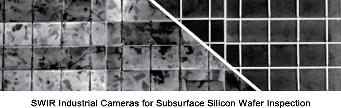
SWIR Industrial Cameras for Subsurface Silicon Wafer Inspection
Silicon lets through short wave infrared or SWIR light between about 900 and 1700 nanometers, which means special SWIR cameras can see what's going on underneath the surface without damaging anything. These cameras catch all sorts of hidden problems that regular visible light systems miss completely, including tiny cracks, empty spaces inside materials, and unwanted chemical impurities. For manufacturers working with cutting edge technology nodes, this kind of imaging tackles major issues such as interference from thin films and contamination on the backside of silicon wafers. When using SWIR inspection techniques, factories report around 30 percent fewer false alarms compared to just looking at surfaces alone. Plus these systems keep up with production demands handling over 200 wafers per hour. Best part? They don't harm the wafers during inspection so engineers can adjust processes in real time without having to cut them open for analysis.
Balancing Inspection Accuracy and Throughput: Mitigating False Positives in High-Speed Industrial Camera Systems
The semiconductor industry needs industrial cameras capable of spotting defects at the micron level while still keeping up with production speeds that often hit over 1,000 units every minute. But there's a catch when these lines run faster. The system becomes more prone to false alarms where it incorrectly identifies something as defective. These mistakes aren't just annoying they actually cost money. According to industry numbers, one recurring false positive signal can drain around $740,000 each year from companies through wasted time fixing non-existent problems, production stoppages, and throwing away perfectly good components that were mistakenly flagged.
To resolve this tension, leading systems integrate three complementary strategies:
- Adaptive AI algorithms, continuously refined using live production data to distinguish true defects from environmental noise (e.g., vibration artifacts or specular glare);
- Multi-spectral imaging, which mitigates reflectivity-induced false readings by analyzing substrate behavior across wavelengths;
- Hardware-accelerated processing via FPGAs, enabling real-time analytics at >10 Gpx/sec to sustain speed without sacrificing sensitivity.
Precision-tuned sensitivity thresholds–calibrated per process step and material stack–reduce false positives by over 30% while meeting throughput targets. The result is fewer unwarranted stoppages, less scrapping of functional components, and tighter alignment between inspection rigor and operational efficiency.
Ready to Optimize Your Electronics & Semiconductor Inspection with Industrial Cameras?
Electronics and semiconductor manufacturing requires industrial camera solutions that offer uncompromising micron-scale precision, real-time processing, and high throughput. All these should address the unique challenges of wafer, IC, and PCB production, from subsurface defect detection to cleanroom edge monitoring. Cutting corners on camera performance or specialized technology results in reduced yields, costly false positives, and unplanned downtime, which undermines the efficiency and quality of semiconductor and electronics workflows.
With 15 years of machine vision expertise, HIFLY Technology provides tailored industrial camera solutions for electronics and semiconductor manufacturing. These include high-resolution global shutter cameras, multi-spectral fusion systems, and SWIR specialized cameras. They are paired with matching industrial lenses and machine vision lighting for a seamless, integrated inspection system. Backed by ISO 9001:2015 certification and global technical support, our solutions are in line with the zero-defect, high-throughput goals of your semiconductor and electronics production lines.
Contact us today for a no-obligation consultation to design an industrial camera inspection solution that meets your precise manufacturing needs.